Bipolar And Unipolar Logic Families
Logic Families
In digital electronics, the circuits that are used to build logic gates (such as AND, OR, NOT, etc.) are called Logic Families.
Bipolar Logic:
It uses BJT (Bipolar Junction Transistor). In this type, two types of charge carriers (electrons and holes) work together. As a result, it offers good speed, but it consumes more power and generates more heat. In the old days, TTL was very popular.
Unipolar Logic:
It uses MOSFET. Here, only one type of charge carrier (either electrons or holes) is involved. Because of this, power consumption is much lower, and more circuits can be fabricated in the same area. Nowadays, CMOS is the most widely used because it is ideal for battery-powered devices (such as mobiles and laptops).
Difference Between Bipolar and Unipolar Logic Families at a Glance
| Feature | Bipolar Logic | Unipolar Logic |
|---|---|---|
| Type of Transistor | BJT (NPN/PNP) | MOSFET |
| Charge Carriers | Both Electrons and Holes | Only Electrons or Only Holes |
| Power Consumption | High | Very Low |
| Speed | Very Fast | Relatively Lower |
| Density (No. of circuits per chip) | Low | Very High |
| Examples | TTL, ECL | CMOS, NMOS |
CMOS (Complementary Metal-Oxide-Semiconductor)
It is widely used because it consumes very little power, can pack billions of transistors in a small space, and is highly reliable.
CHARACTERISTICS OF DIGITAL ICs
With the widespread use of ICs in digital systems and the development of various fabrication technologies, it has become essential to be familiar with the characteristics of IC logic families. ICs are categorized based on their “complexity,” .
IC Classification by Integration Level
| Type of IC | Number of Equivalent Gates | Number of Components |
|---|---|---|
| SSI (Small-Scale Integration) | Less than 12 | Up to 99 |
| MSI (Medium-Scale Integration) | 12 – 99 | 100 – 999 |
| LSI (Large-Scale Integration) | 100 – 999 | 1,000 – 9,999 |
| VLSI (Very Large-Scale Integration) | Above 1,000 | Above 10,000 |
Performance Characteristics of Digital ICs
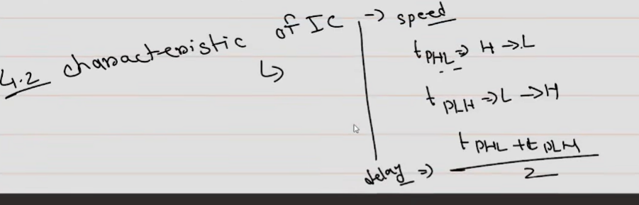
Speed of Operation: Determined by the propagation delay; it is the time taken for a change at the input to reflect at the output.
Power Dissipation: The amount of power consumed by the gate, which is dissipated as heat. $$P = V_{CC} \times I_{CC}$$
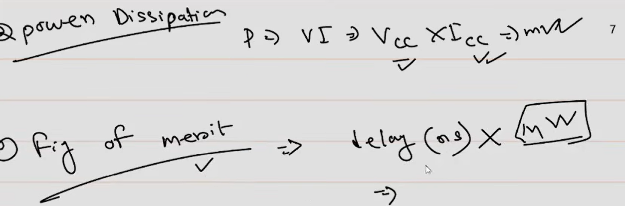
Figure of Merit: Calculated as the product of propagation delay and power dissipation ($Speed \times Power$). A lower value indicates better efficiency.
$\text{Figure of merit} = \text{propagation delay time } (ns) \times \text{power } (mW)$
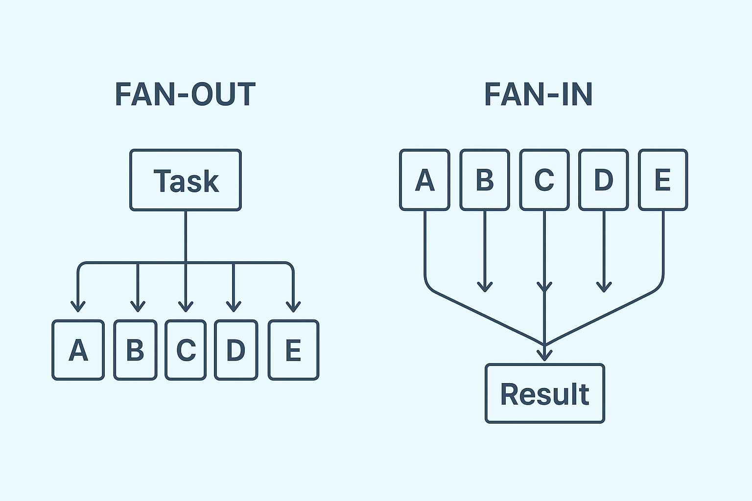
Fan-out: is the maximum number of simillar gates that one single gate can provide power to at the same time.
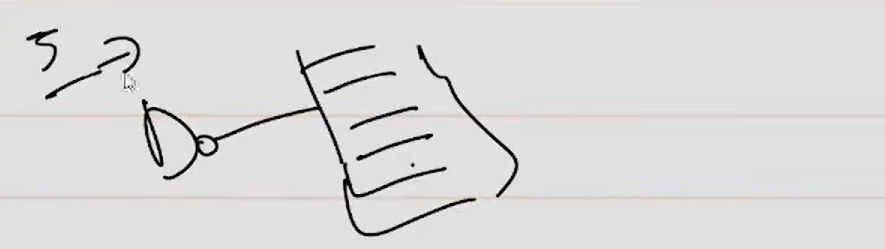
Advantage: The higher the fan-out, the more gates you can drive without needing additional driver circuits. This significantly reduces the overall complexity of the circuit.
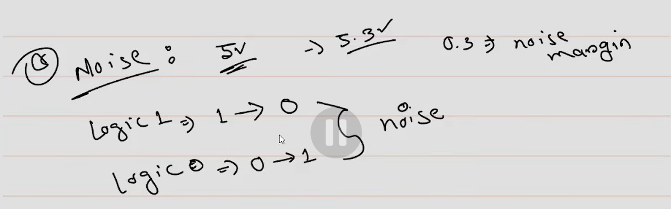
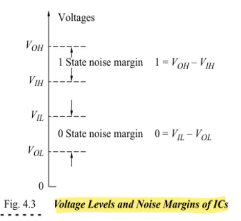
- Noise Immunity: The ability of a circuit to tolerate unwanted electrical interference (noise) without changing the output state.
- Operating Temperature Range: The temperature limits within which the IC can function reliably (e.g., $0$ to $70$°C for commercial use).
- Power Supply Requirements: The specific voltage levels and stability required for the IC to operate (e.g., $5V$ or $3.3V$).
- Fan-in: The number of inputs a single logic gate can handle. Alternatively, Flexibility refers to the chip’s ability to interface with other logic families.
10.Flexibilities Available Several types of flexibility or advantages are considered. These include:
- The Breadth of the Series: This refers to the variety of logic functions—such as
different types of gates, flip-flops, and counters—available within a single series.- Popularity of the Series: The cost of an IC depends on its popularity. When ICs are produced in massive quantities, the unit price decreases, and they become easily available from multiple manufacturers (multi-sourcing).
- Wired-Logic Capability: This allows the outputs of ICs to be connected directly to perform additional logic functions (like Wired-AND or Wired-OR) without the need for extra hardware or gates.
- Availability of Complement Outputs: Many ICs provide both the original signal and its inverted (complement) signal at the output. This eliminates the need for an external inverter or NOT gate.
Bipolar Logic
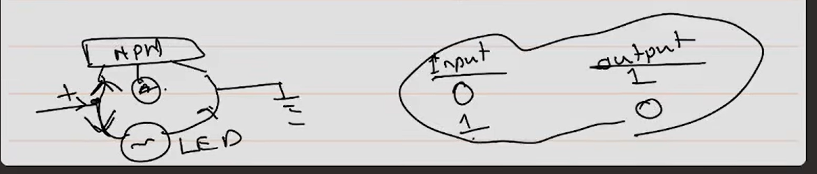
Implement Not gate using transsistor
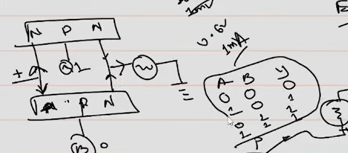
Implement OR gate (Two transistor connected in parallel) using transsistor
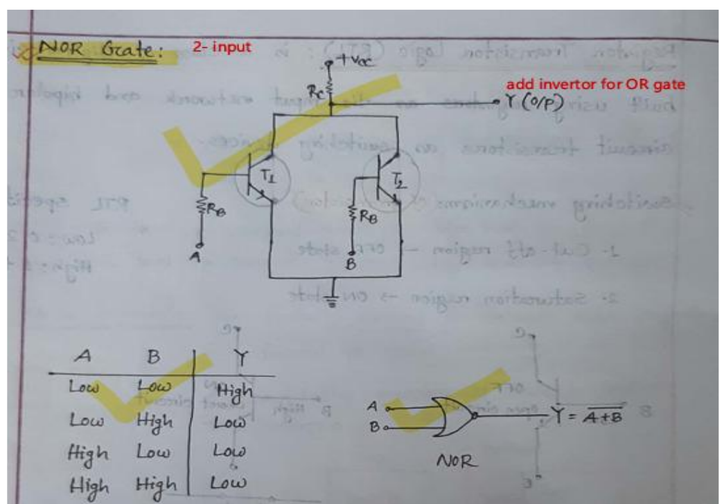
Implement NOR gate using transsistor
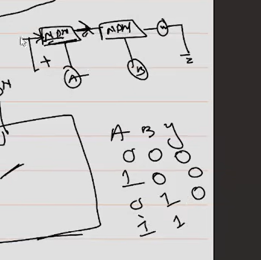
Implement AND gate using transsistor
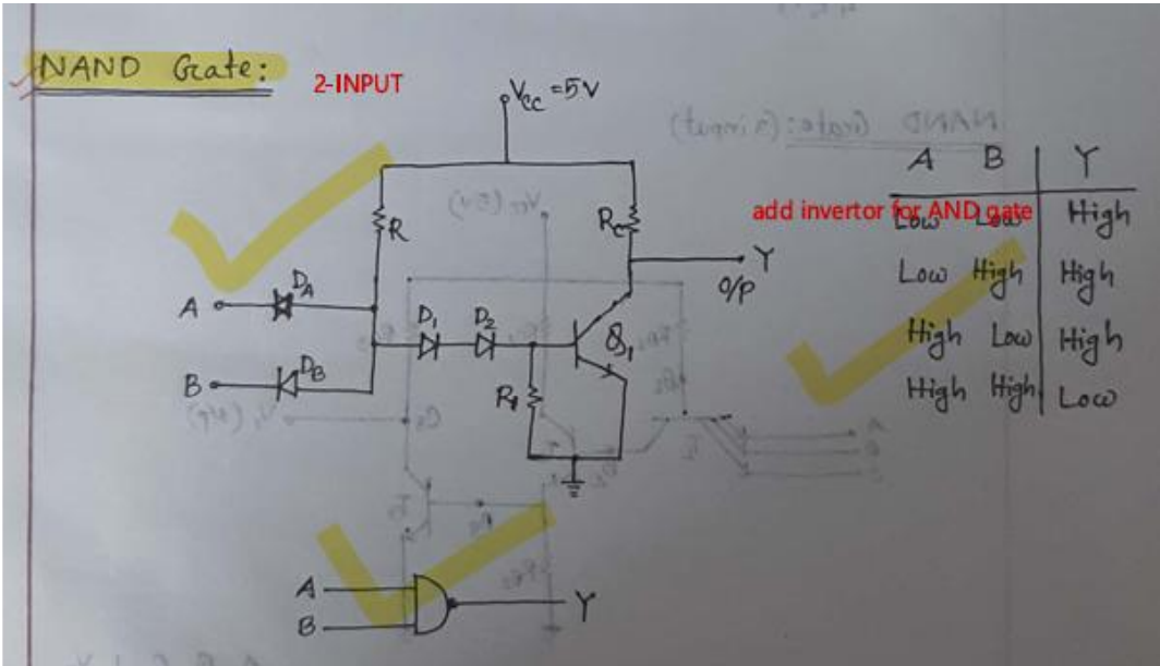
Implement NAND gate using transsistor
Resistor-Transistor Logic (RTL)
RTL was the most popular logic family used in digital systems. As the name suggests, it is primarily constructed using resistors and transistors. While it is rarely used in modern high-speed electronics, it remains fundamental for understanding the basic concepts of digital logic gates.
Key Characteristics of RTL:
- Basic Gate: The fundamental (basic) gate of the RTL family is the NOR gate.
- Structure: a 2-input RTL NOR gate driving $N$ number of similar gates.
- Fan-in: This refers to the number of input terminals a gate has. Since the circuit in the image has inputs $A$ and $B$, the Fan-in is 2.
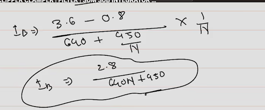
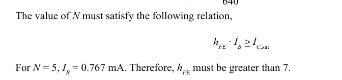
IB value must be greater than N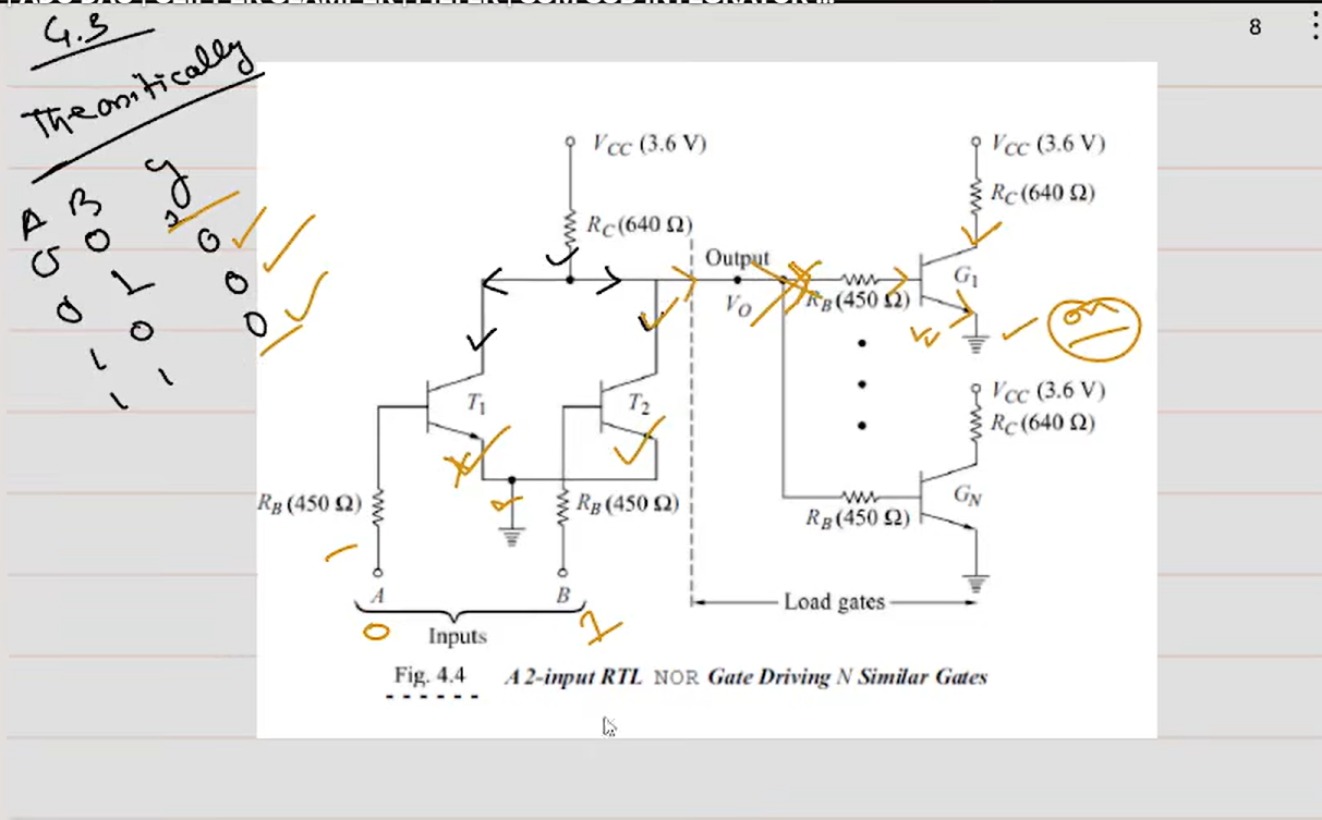
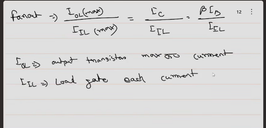
Fanout in RTL
Circuit Operation
- The circuit consists of two transistors, $T_1$ and $T_2$, connected in parallel.
- If input $A$ OR input $B$ (or both) is HIGH (Logic 1), the corresponding transistor turns ON (enters saturation). This pulls the output $V_O$ down to the ground, resulting in a LOW (Logic 0) output.
- The output is HIGH (Logic 1) ONLY when both inputs $A$ and $B$ are LOW (Logic 0). In this state, both transistors are OFF (cutoff), and the output is pulled up to $V_{CC}$.
Circuit Operation (Step-by-Step): Imagine you have a battery supplying 3.6 V.
- When both inputs are LOW ($A=0, B=0$):
- You are not applying any voltage to the bases of transistors $T_1$ and $T_2$.
- Both transistors act like “open switches.”
- Since the current has no path to flow to the ground, the voltage from $V_{CC}$ goes directly to the output.
- Result: Output is HIGH (approximately 3.6 V).
- When any one input is HIGH ($A=1$ or $B=1$):
- Suppose you apply voltage to input $A$. This causes transistor $T_1$ to act like a “closed switch.”
- The current coming from $V_{CC}$ now flows through $T_1$ directly to the Ground.
- Because the output terminal is now effectively connected to the ground, the voltage drops to nearly zero.
- Result: Output is LOW (approximately 0.2 V).
In Simple Terms: This circuit follows the NOR gate truth table: if any input is 1, the output is 0.
Loading Considerations.
This calculation tells us the maximum number of gates ($N$) that an RTL gate can drive while ensuring the transistors continue to switch correctly. This is known as Loading Considerations.
4.3.3 Noise Margins
Noise margin is the measure of a gate’s ability to tolerate electrical interference. It defines how much unwanted voltage (“noise”) can be added to a signal before the gate produces an incorrect result.
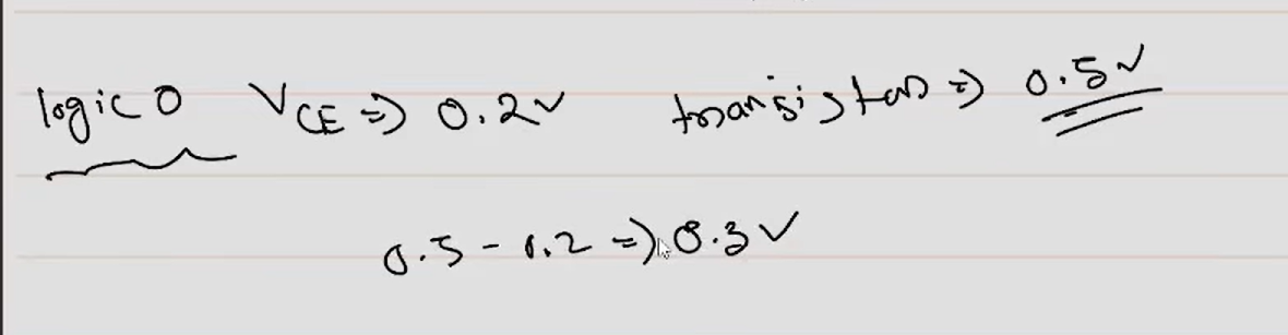
- Logic 0 Noise Margin ($\Delta 0$): When the output is LOW (0), the voltage is approximately $0.2\text{ V}$. If external noise pushes this voltage up to $0.5\text{ V}$ (the cut-in voltage of the transistor), the next transistor might accidentally turn on. Therefore, the noise margin for Logic 0 is: $0.5\text{ V} - 0.2\text{ V} = 0.3\text{ V}$.
- Logic 1 Noise Margin ($\Delta 1$): This depends on the number of load gates ($N$). According to the calculations, if $N=5$, the output voltage is $1.14\text{ V}$. Since the next gate requires at least $1.04\text{ V}$ to stay “ON” (Logic 1), the margin is very slim: only $0.1\text{ V}$ ($1.14\text{ V} - 1.04\text{ V}$).
4.3.4 Propagation Delay Time
Propagation delay is the time it takes for a signal to travel from the input to the output. In RTL, this is heavily influenced by the fan-out ($N$).
Current Source Logic
RTL is categorized as Current Source Logic because:
- When the output is at Logic ‘1’ (HIGH), the gate provides (sources) current to the load transistors.
- Since this sourced current is significantly higher than any leakage current, it is characterized as a current source.
Wired-Logic (Implied-AND)
When the outputs of two or more gates are connected directly together with a wire, the resulting configuration is called Wired-Logic or Implied-AND.
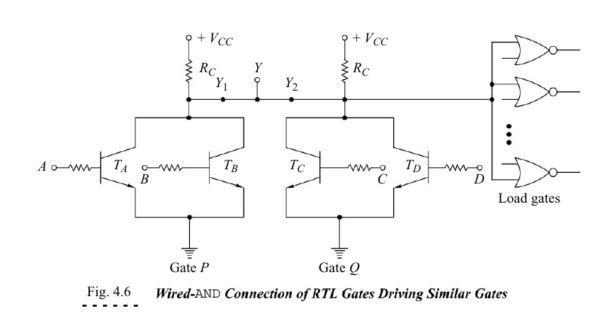
- The outputs of two separate NOR gates ($Y_1$ and $Y_2$) are tied together.
- Output of the first gate: $Y_1 = \overline{A+B}$
- Output of the second gate: $Y_2 = \overline{C+D}$
- The final combined output becomes: $Y = Y_1 \cdot Y_2 = (\overline{A+B}) \cdot (\overline{C+D})$
Applying De Morgan’s Theorem, this can also be expressed as: $$Y = \overline{(A+B) + (C+D)} = \overline{A+B+C+D}$$
Advantage: You can increase the number of inputs (Fan-in) of a logic function without using an additional physical AND gate. However, keep in mind that this type of connection can negatively affect the Fan-out and the overall operating speed of the circuit.
Summary of RTL Logic Family Characteristics
Based on the complete discussion, here are the defining features (and weaknesses) of Resistor-Transistor Logic (RTL):
- Poor Noise Margin: It is highly sensitive to electrical noise (as low as $0.1\text{ V}$ for Logic 1), which can lead to incorrect outputs.
- Poor Fan-out Capabilities: It cannot drive a large number of subsequent gates effectively.
- Low Speed: Compared to modern ICs, RTL is very slow due to the charging time of its passive pull-up resistors.
- High Power Dissipation: It consumes a significant amount of electrical energy, which is wasted as heat.
Diode-Transistor Logic (DTL) (video 1.38 minute)
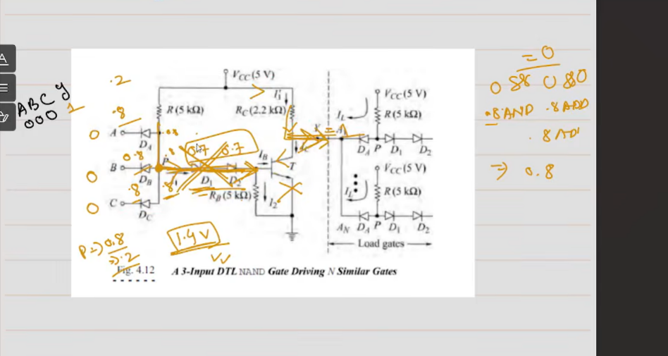
NAND gate, here is the English explanation of where the output is located and how it functions:
1. Where is the output located?
In the circuit diagram, the output terminal $Y$ is connected directly to the Collector pin of the transistor.
- This terminal is connected to the positive power supply $V_{CC}$ (typically 5V) through a collector resistor $R_C$ (usually $2.2\text{ k}\Omega$).
- At the same time, this collector pin is waiting to be connected to the Ground through the transistor’s emitter once the transistor is switched on.
2. How does the output work?
The state of the output (HIGH or LOW) depends on whether the transistor is acting as an open or closed switch:
Case 1: Output is HIGH (Logic 1)
- When any input is LOW, the diodes conduct in a way that keeps the transistor in the OFF (Cut-off) state.
- Since the transistor is “closed” to the ground, the output terminal $Y$ has no path to the ground.
- Current from $V_{CC}$ flows through $R_C$ directly to the output.
- Result: You get a Logic 1 (approximately 5V) at the output.
Case 2: Output is LOW (Logic 0)
- When all inputs are HIGH, the diodes are reverse-biased, allowing current to flow into the base of the transistor, turning it ON (Saturation).
- The turned-on transistor acts like a short-circuit switch to the ground.
- The output terminal $Y$ is now directly connected to the Ground through the transistor.
- Result: The output voltage drops to near zero (approximately 0.2V), which is Logic 0.
Propagation Delays
Propagation delay is the time required for a transistor to switch between its ON and OFF states.
- Turn-on Delay: When the transistor turns on, the output capacitance discharges very quickly through the low-resistance path of the transistor. Therefore, this delay is relatively short.
- Turn-off Delay: When the transistor turns off, the output capacitance must charge through the collector resistor ($R_C$). This is a slower process. Typically, the turn-off delay is 2 to 3 times longer than the turn-on delay.
- Average Delay: For a standard DTL gate, the propagation delay ranges from 30 to 80 nanoseconds (ns).
Current Sink Logic
DTL is categorized as Current Sink Logic because:
- When the output is HIGH (1), the gate provides (sources) only a very small amount of current to the load.
- When the output is LOW (0), the output transistor is saturated and acts as a path to the ground. It “sinks” (absorbs) a large amount of current coming from the load gates and sends it to the ground.
- Since the capacity to sink current is significantly higher than its ability to source current, it is called Current Sink Logic.
Wired-Logic
When the outputs of two NAND gates are connected directly via a wire without using an additional physical gate, it is called Wired-AND or Implied-AND.
Circuit Analysis
- The final output ($Y$) will be HIGH (1) only if the outputs of both individual gates are HIGH ($Y_1=1, Y_2=1$).
- If either gate output goes LOW (0), the final output $Y$ becomes LOW (0) because that transistor pulls the entire line to the ground.
- Mathematical Expression: $$Y = Y_1 \cdot Y_2 = (\overline{A \cdot B}) \cdot (\overline{C \cdot D}) = \overline{AB + CD}$$
table
| Transistor State | Output $Y$ Connected to: | Logic Level |
|---|---|---|
| OFF (Cut-off) | $V_{CC}$ (5V) | HIGH (1) |
| ON (Saturation) | Ground (0V) | LOW (0) |
In simple terms: When the transistor turns on, it “pulls” the output down to the ground. This creates a NAND logic function because the output only goes LOW when all inputs are HIGH.
3-input Transistor-Transistor Logic (TTL) NAND Gate.
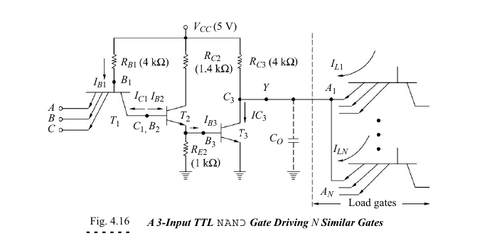
Key Components of a TTL(Multi-amitter transistor) NAND Gate
1. Multi-Emitter Transistor ($T_1$)
The heart of the TTL gate is the multi-emitter transistor ($T_1$). In this specific circuit, it has three emitters (labeled A, B, and C), which serve as the inputs. This design allows multiple inputs to be processed by a single transistor, a hallmark of TTL technology.
2. Circuit Stages
- Input Stage ($T_1$): Receives the logic signals from inputs A, B, and C.
- Phase Splitter ($T_2$): This transistor splits the signal to drive the output stage efficiently, ensuring that the output transistors switch correctly.
- Output Stage ($T_3$): Acts as an inverter. It provides the final output ($Y$) and handles the current drive for the load.
- Resistors: $R_{B1}$ ($4\text{ k}\Omega$), $R_{C2}$ ($1.4\text{ k}\Omega$), $R_{E2}$ ($1\text{ k}\Omega$), and $R_{C3}$ ($4\text{ k}\Omega$) are used for biasing and limiting current to protect the transistors.
Theory of Operation (NAND Logic)
A NAND gate follows the rule: The output is ‘Low’ only when all inputs are ‘High’; otherwise, the output is ‘High’.
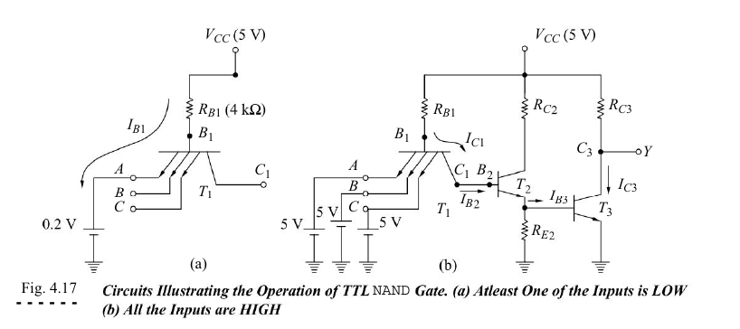
Case 1: All Inputs are High (Logic 1)
When A, B, and C are all connected to a High voltage, the emitter-base junctions of $T_1$ are reverse-biased(becaused $V_{cc}$ is 5 V that protect flow the input high voltage(5 v) form the input ). The current from $V_{CC}$ flows through the base-collector junction of $T_1$ into the base of $T_2$ and subsequently $T_3$. This turns $T_3$ ON (Saturation), pulling the output $Y$ down to ground level.
- Output $Y$ = Logic 0 (Low)
Case 2: Any Input is Low (Logic 0)
If at least one input (A, B, or C) is grounded or Low, the corresponding emitter-base junction of $T_1$ becomes forward-biased. The current flows through $T_1$ to the Low input(using ground) instead of reaching the base of $T_2$. Consequently, $T_2$ and $T_3$ turn OFF (Cut-off). The output $Y$ is then pulled up to $V_{CC}$ (because $T_3$ transistor is cut-off and then ($V_{cc}$ direc connect the output $Y$ that no ground connection because {T_3} is off)).
- Output $Y$ = Logic 1 (High)
“There is no electron flow in the base of $T_2$. If there is no current at the base of a transistor, it will not conduct any current even if its collector is connected to $V_{CC}$. In this state, it acts as an open switch or is in the ‘Cut-off’ state.”
Fan-out and Loading
The dotted section on the right side of your diagram illustrates Fan-out.
- Definition: Fan-out represents the maximum number of similar digital inputs that the output of a single gate can reliably drive.
- In the diagram, the output $Y$ is driving $N$ number of gates ($I_{L1}$ to $I_{LN}$). If $N$ exceeds the rated Fan-out, the voltage levels may drop, leading to logic errors.
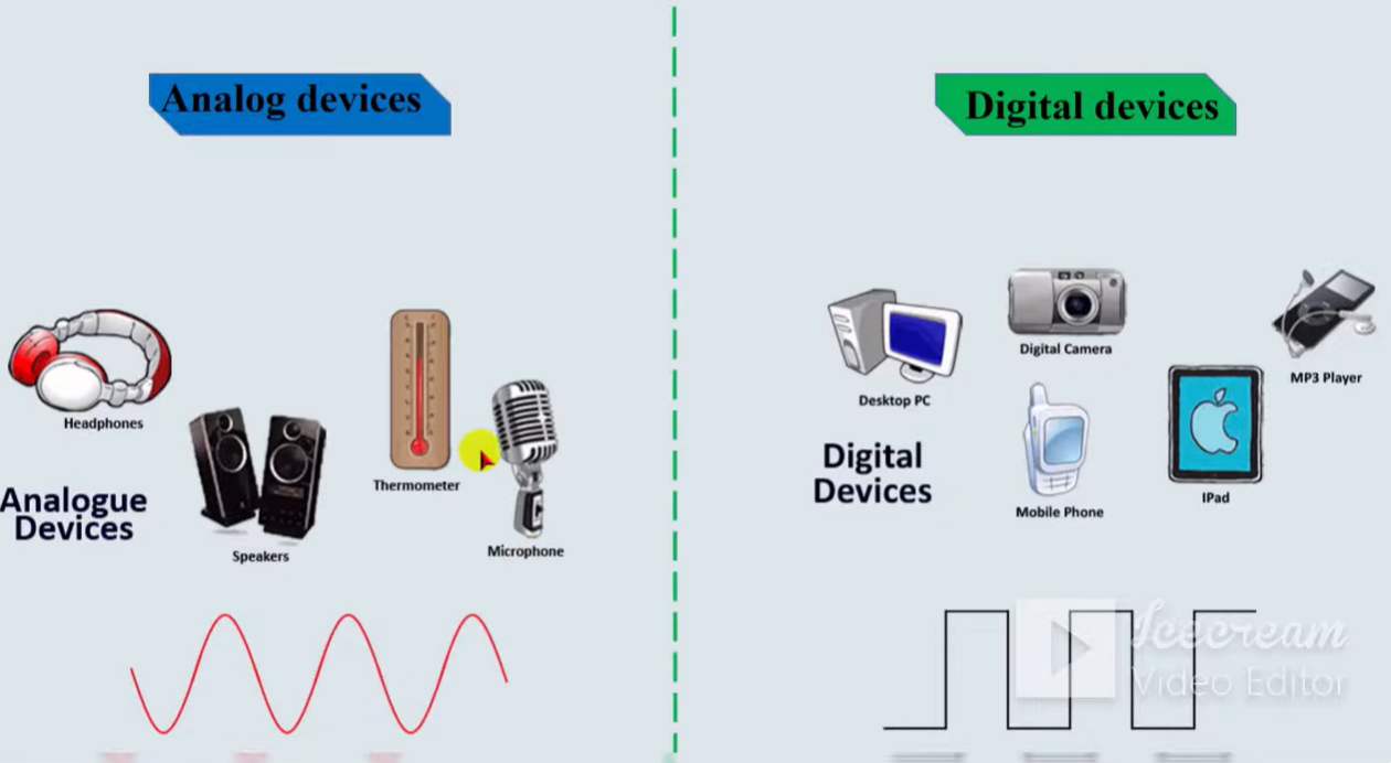
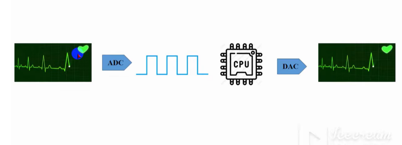
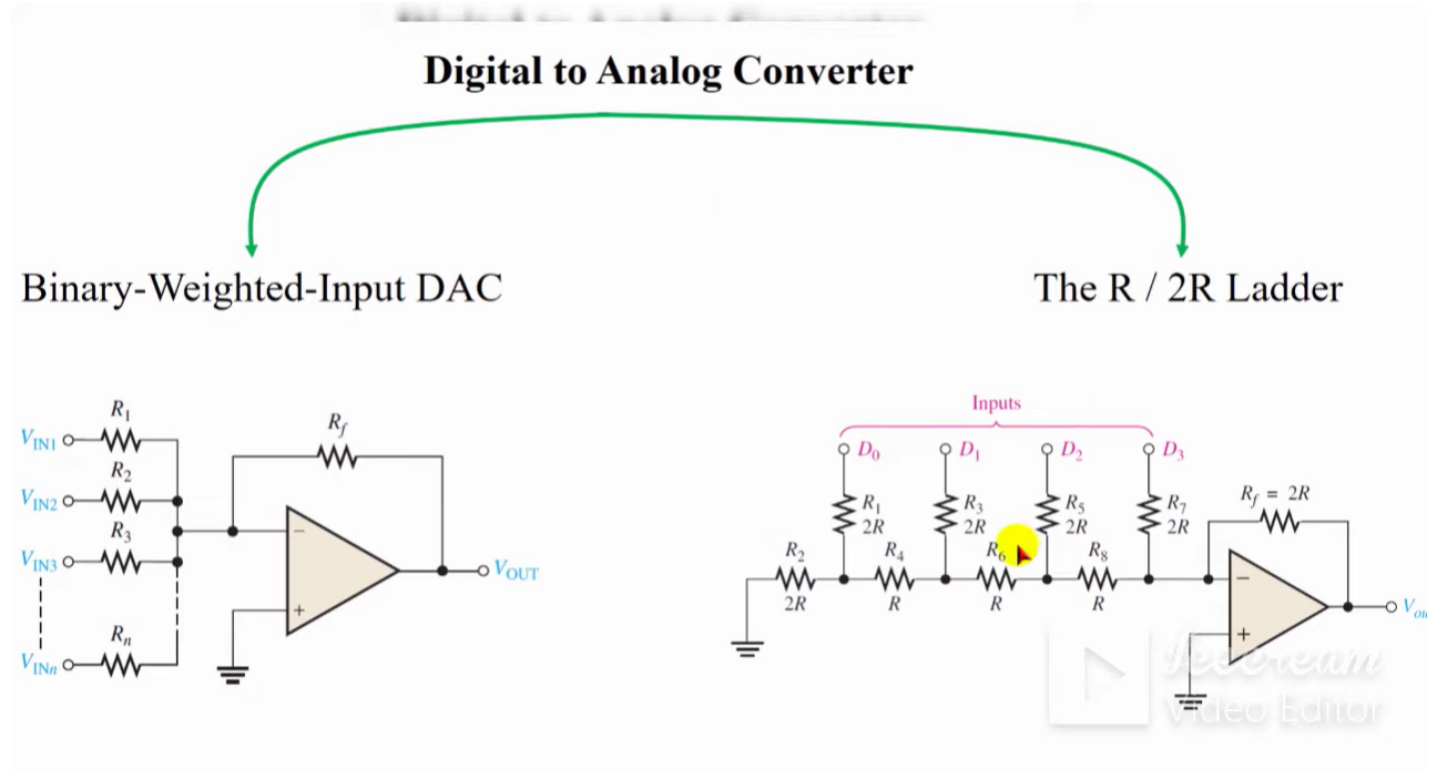
A/D (Analog-to-Digital)
কোয়ান্টাইজেশন এবং এনকোডিং হলো একটি গন্তব্যে যাওয়ার "নিয়ম" বা পদ্ধতি, আর ফ্ল্যাশ এডিসি হলো সেই গন্তব্যে যাওয়ার জন্য ব্যবহার করা বিশ্বের "দ্রুততম গাড়ি"।
Steps to Convert Analog Signals to Digital
To convert a continuous analog voltage into a digital format, the signal must pass through these four primary stages:
- samplingTaking “snapshots” or samples of a continuous analog signal at specific, regular time intervals with respect to amplitude.
- Holding: Keeping the sampled voltage level steady for a short period so the system has enough time to process it. These two steps are usually handled by a Sample-and-Hold (S/H) circuit.
- Quantizing: Mapping the sampled voltage to the nearest predefined digital voltage level (for example, rounding a 4.99V signal to a solid 5V level).
- Encoding: Converting the quantized value into a binary code (a sequence of 0s and 1s) that a computer can store and process.
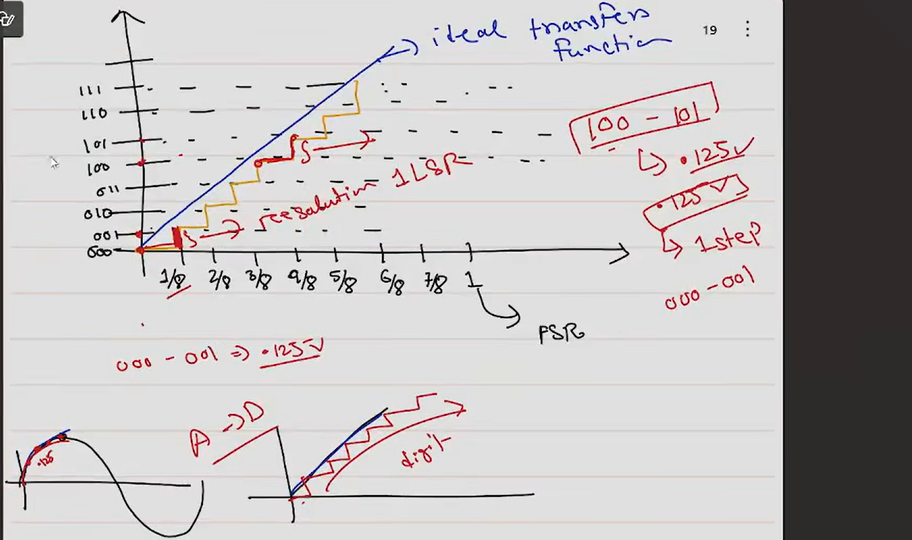
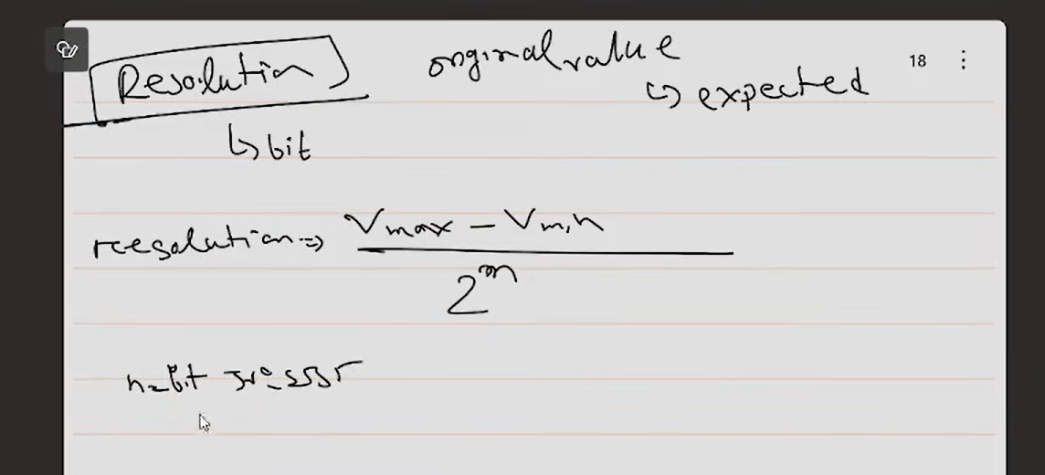
- Resolution/ step-size in ADC refers to how many small steps or divisions a system can use to represent an analog signal. The higher the resolution, the more closely the digital signal resembles the original analog source.
Measurement: It is expressed in Bits. A higher bit-depth means more levels ($2^n$).
- Example: A 10-bit resolution has $2^{10} = 1024$ steps, while a 12-bit resolution has $2^{12} = 4096$ steps.
The Rule: High Resolution = More Steps = Greater Precision/Accuracy.
Step-by-Step ADC: A Real-World Example
we are recording a voice where the maximum voltage is $5\text{V}$.
1. Sampling
This involves measuring the height (amplitude) of the analog signal at specific time intervals.
- Example: If you measure the signal every 1 second, you might get:
- Sec 1: $1.26\text{V}$
- Sec 2: $3.42\text{V}$
- Sec 3: $4.89\text{V}$
- Sec 4: $2.15\text{V}$
2. Quantization
Analog values are often complex decimals ($1.26$, $3.42$, etc.), but digital systems cannot store infinite precision. We round these values to the nearest predefined “Level.”
- Example: In a system with 8 levels (0 to 7):
- $1.26\text{V} \rightarrow \textbf{Level 1}$
- $3.42\text{V} \rightarrow \textbf{Level 3}$
- $4.89\text{V} \rightarrow \textbf{Level 5}$
- $2.15\text{V} \rightarrow \textbf{Level 2}$
3. Encoding
In the final step, these level numbers are converted into binary code (0s and 1s). Since we have 8 levels, we use 3-bit encoding ($2^3 = 8$).
- Example:
- Level 1 $\rightarrow$ 001
- Level 3 $\rightarrow$ 011
- Level 5 $\rightarrow$ 101
- Level 2 $\rightarrow$ 010
Why the Math Matters: Levels and Bits
Your understanding of the 8 levels is perfectly correct. Digital systems use binary powers. To get 8 distinct levels, you need 3 bits because: $$2^3 = 8$$
If you move to a $5\text{V}$ system with 8 levels, each “step” or resolution is: $$\text{Resolution} = \frac{5\text{V}}{8} = 0.625\text{V}$$
“If any voltage falls within the range of $0\text{V}$ to $0.624\text{V}$, the system will categorize it as Level 0 (000). If the voltage falls between $0.625\text{V}$ and $1.24\text{V}$, the system will categorize it as Level 1 (001).”
2. The Rounding Process
The quantizer establishes boundaries for the signal. For example, if your 3-bit system has a step size of 1V:
- If the input is $2.4\text{V}$, the quantizer rounds it down to the nearest level: $2\text{V}$.
- If the input is $2.6\text{V}$, the quantizer rounds it up to: $3\text{V}$.
This process of forcing a continuous value into the nearest predefined “bucket” or integer is the essence of quantization.
3. Quantization Error ($e_q$)
Since we are rounding off the actual voltage, some information is inevitably lost. This loss is known as Quantization Noise or Error.
Formula: $$e_q = V_{actual} - V_{quantized}$$
As per the technical standards in your text, the maximum error is typically kept within $\pm \frac{1}{2} \text{LSB}$. This means the digital representation will never deviate from the actual analog value by more than half of a single step.
4. Why Increase the Bit Depth?
If we upgrade from 3-bit to 8-bit or 16-bit:
- More Levels: A 16-bit system has $65,536$ levels compared to just $8$ levels in a 3-bit system.
- Smaller Step Size: Smaller steps mean the “rounding” is much more precise, significantly reducing the Quantization Error.
- Result: You get high-fidelity, noise-free sound or high-resolution images.
Why do we need Sample-and-Hold (S/H)?
Analog signals (like sound or voltage) change continuously. When converting these to digital, an ADC (Analog-to-Digital Converter) requires a specific amount of time to complete its process, known as Conversion Time.
- The Problem: If the input voltage fluctuates while the ADC is mid-conversion, the resulting digital output will be inaccurate or “noisy.”
- The Solution: The Sample-and-Hold circuit. It captures the voltage at a precise moment (Sample) and keeps it steady (Hold) until the ADC finishes its job.
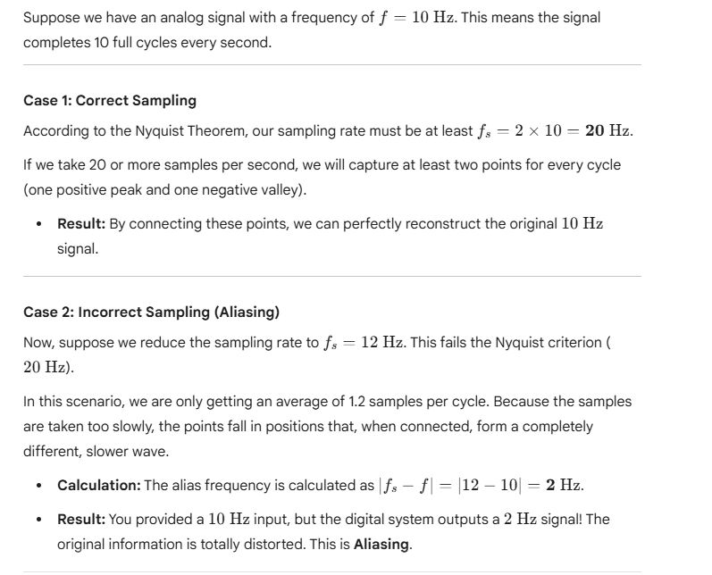
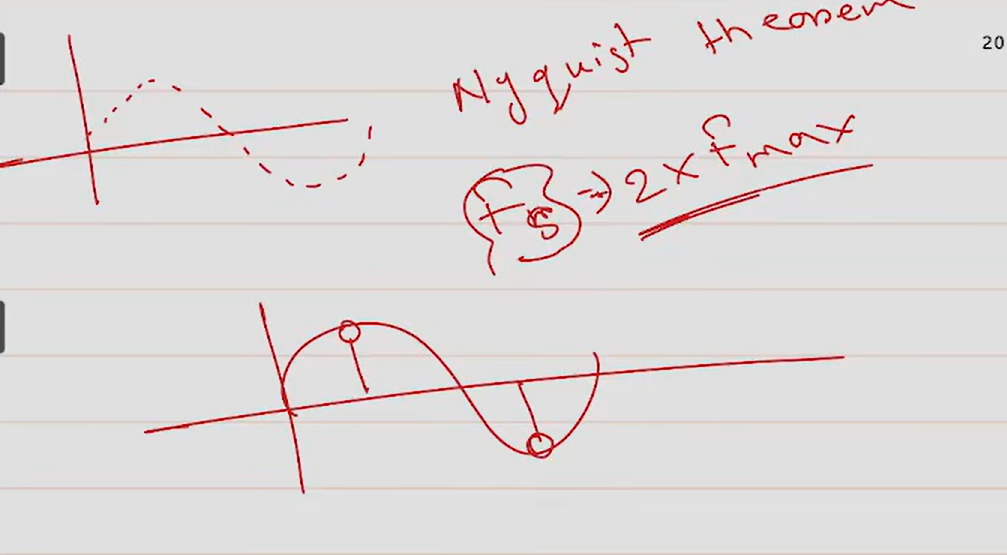
The Sampling Theorem (Nyquist Criterion)
As noted in your image, the mathematical formula is: $$f_s \geq 2f$$
- $f$: The highest frequency component in your analog signal.
- $f_s$: The sampling rate (samples taken per second).
How the S/H Circuit Works
An ideal Sample-and-Hold circuit consists of two main components:
- Electronic Switch: A high-speed switch that closes briefly during the sampling interval ($T_s$).
- Holding Capacitor: When the switch closes, this capacitor charges to the input voltage level. When the switch opens, the capacitor retains (holds) that charge, providing a steady voltage to the ADC.
Practical Application: Digital Audio Example
Imagine you are recording a song with a maximum frequency of $20,000 \text{ Hz}$.
- Required Sampling Rate ($f_s$): According to the theorem, $f_s \geq 2 \times 20,000$, which is $40,000 \text{ samples/sec}$. (Standard CDs use $44.1 \text{ kHz}$ for this reason).
- Sampling Interval ($T_s$): The time between samples would be $T_s = 1/f_s \approx 22.67 \text{ microseconds}$.
- The Holding Phase: If the ADC takes $10 \text{ microseconds}$ to convert a sample, the S/H circuit ensures the voltage (e.g., $3.5\text{V}$) remains frozen for those $10 \text{ microseconds}$, preventing the ADC from seeing the signal’s natural drift during processing.
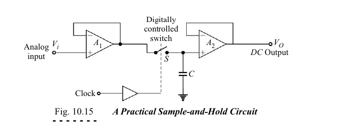
Practical Sample-and-Hold (S/H) Circuit.
This design is a significant improvement over a simple switch-capacitor circuit because it addresses real-world issues like signal distortion and voltage drop.
The Role of the Two Op-Amps ($A_1$ and $A_2$)
This circuit uses two Unity Gain Buffer Amplifiers to isolate the storage capacitor and ensure precision.
- Buffer $A_1$ (Input Side): This amplifier has a very high input impedance, meaning it doesn’t “load” or drain the analog input source. Its low output impedance allows it to provide enough current to charge the holding capacitor almost instantly the moment the switch closes.
- Buffer $A_2$ (Output Side): This amplifier acts as a “guard” for the capacitor. Because its input impedance is nearly infinite, it prevents the charge stored in the capacitor from leaking out. This ensures the voltage remains rock-steady until the ADC completes its conversion.
The Digitally Controlled Switch
The switch in the center (typically a MOSFET) is controlled by a digital clock signal.
- Sample Mode: When the clock pulse is High, the switch closes. The capacitor $C$ charges to the current value of the analog input voltage via $A_1$.
- Hold Mode: When the clock pulse is Low, the switch opens. The capacitor is now isolated, “freezing” the voltage level.
Capacitor Selection (Teflon or Polycarbonate)
The textbook highlights a critical detail: the choice of dielectric material for the capacitor.
- The Problem: Standard capacitors suffer from Dielectric Absorption or leakage, where the stored voltage slowly “droops” or fades over time.
- The Solution: Capacitors with Teflon or Polycarbonate dielectrics are used because they have extremely low leakage rates. This is vital because if the voltage drops even slightly during the “Hold” phase, the ADC will produce an incorrect digital value.
Operational Summary
- Sampling: Switch $S$ closes $\rightarrow$ Capacitor $C$ charges rapidly through $A_1$.
- Holding: Switch $S$ opens $\rightarrow$ High input impedance of $A_2$ prevents the charge from escaping.
- Output: A stable DC voltage $V_O$ is delivered to the ADC for processing.